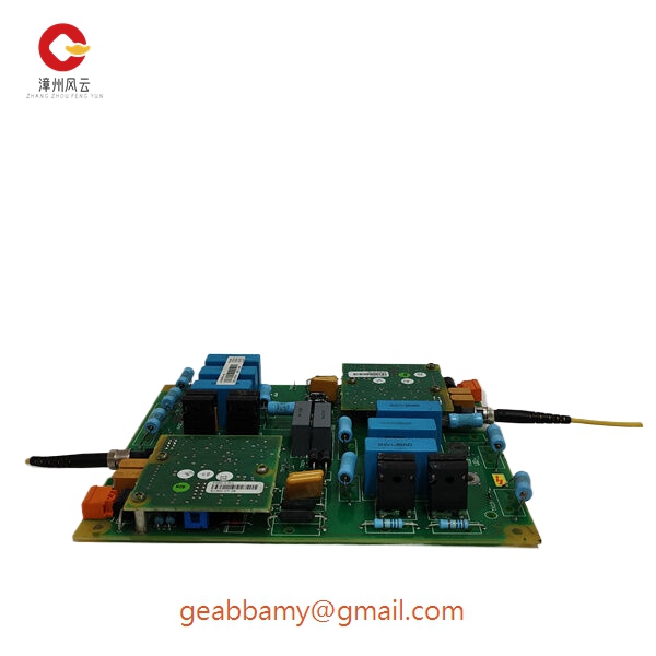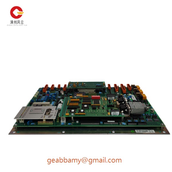

📣Model Number:IW93 HESG440356R1
🌍Country of origin: USA France Germany Estonia Norway UK
⌚Delivery date: in stock
🛠After-sales service: brand new with one year warranty
⚙️ Product Category: Module/Controller/Server/Motor/Touch Screen
🕰Warranty: 12 months/365 days
☎️ Please contact me: 15359029662 Ms. Amy Sun
📎Chinese official website: www.dcsplcabb.com
📩Email: geabbamy@gmail.com
💬Whatsapp: +86 15359029662


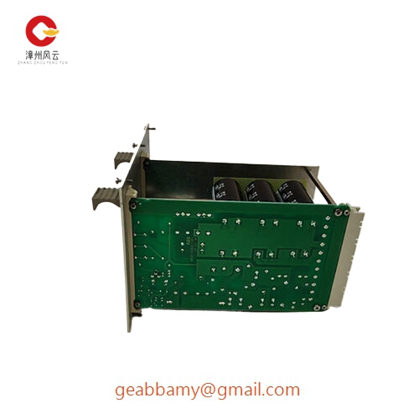
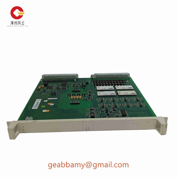
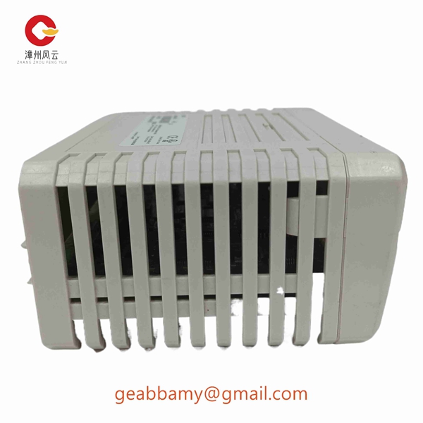
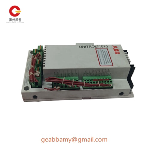
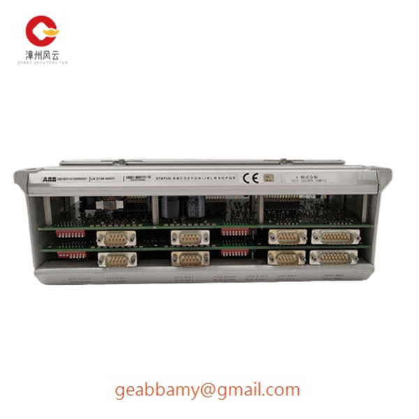
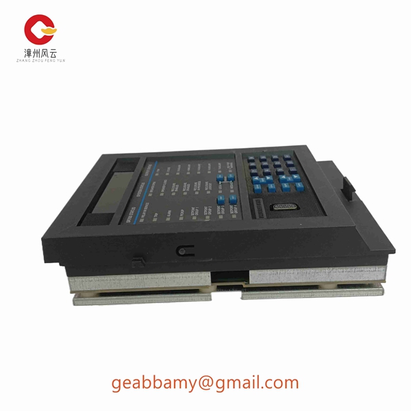
IW93 HESG440356R1
The IW93 HESG440356R1 features eight A/D acquisition IP modules that make it easy to capture and move data. Each IP module can receive data from any of the eight A/Ds or from a test signal generator. A powerful linked-list DMA engine moves A/D data through the PCIe interface in a unique capture gate drive mode. In this mode, the length of the transfer performed by the link definition does not need to be known before the data is acquired; instead, it is controlled by the length of the acquisition gate. This is useful in applications where the acquisition is driven by an external gate and the exact length of that gate is unknown or may vary. Within each A/D acquisition IP module is a DDC IP core. Because of the flexible input routing of the A/D Acquisition IP Module, many different configurations are possible, including one A/D driving all eight DDCs or each of the eight A/Ds driving its own DDC.
The IW93 HESG440356R1 has independent 32-bit tuning frequency settings ranging from DC to A/D sampling frequencies. Each DDC has its own unique extraction settings, supporting up to 8 different output bandwidths. Extractions can be programmed from 2 to 32,768, providing bandwidths from 100 MHz to several kHz to best suit each application. Digital Signal Processing (DSP) performance can be increased by more than 50 per cent while reducing cost, power and weight. As a core feature of the Jade architecture, the FPGA has access to all data and control paths to enable factory-installed functions including data multiplexing, channel selection, data packing, gating, triggering, and memory control. 5 GB of DDR4 SDRAM banks are available for the FPGA for custom applications. 6.4 GB/s of system memory is sustained by the Gen.3 x8 PCIe link. Gen.3 x8 PCIe link can sustain 6.4 GB/s of system memory data transfer. Eight additional gigabit serial channels and LVDS general purpose I/O lines are available for custom solutions.